Pll block diagram diorio cs talks washington homes File:analog pll (block diagram).png Pll simulation error
Schematic diagram of the PLL simulation circuit | Download Scientific
Mạch giải điều chế pll fm Schematic diagram of the pll simulation circuit Pll schematic synthesizer frequency pcb layout matching impedance ghz
Schematic pll shows implementing
Pll circuit diagramPll exciter Pll circuit simulationPll transmitter fm circuit schematic circuits radio am diagram phase loop locked electroschematics beacons low antenna 4w pcb transmisores broadcast.
Schematic block diagram of the pll.Pll tuning Schematic of the pllPll pcb system.

Pll schematic lo pcb diagram fig
1.5 ghz pll frequency synthesizerPll exciter Pll degital arduino stack systemsAm transmitter circuit diagram pdf.
Functional schematic of a standard pll fig. 3 shows an experimentalPll fm circuit detector diagram frequency ic demodulator 565 internal reduce electric current part has do Pll fm transmitter power circuits schematic low circuit rf synthesized broadcast gr next reference postedPhase-locked loop (pll) fundamentals.

Pll module
Fm pll demodulator diagram block circuit using working theorySynthesizer pll schematic circuit frequency seekic basic diagram shown figure Am pll circuit diagram vco ic seekic signalSchematic diagram of the proposed pll..
Pll fm demodulator circuit using xr2212 . design, working priciple, theoryPll fm detector Pll blockSchematic block diagram of the pll.

Pll cadence
Pll schematic diagramPhase locked loops, block diagram,working,operation,design,applications Pll fm transmitter circuitLocked block loops pll.
Pll circuit page 3 : rf circuits :: next.grPll simplified schematic. Phase locked loopPll block diagram.

Pll phase loop locked detector frequency fundamentals
Pll frequency synthesizer cp reference mhz inputPll_am Full-band phase locked loop circuit diagram fast under pll circuitsPll circuit exciter diagram circuits schematic transmitter diy schematics rf signal electronics vco ic control thumbwheel switches digital.
Pll fm transmitter schematic digital tuning watt circuit pira diagram cz rf transmitters 1w diy electronics electronic oscillator mhz gifPhase locked loop ic Lo pll adf4350 – vhfdesignBlock diagram of cmos pll..

File:all degital pll (block diagram-2).png
Pll block diagram analog file commons wikimediaPcb diagram in operating system Pll frequency synthesizer schematic circuitCmos pll.
.


Schematic diagram of the PLL simulation circuit | Download Scientific

PLL_AM - Signal_Processing - Circuit Diagram - SeekIC.com

PLL Exciter

PLL frequency synthesizer schematic circuit - Basic_Circuit - Circuit
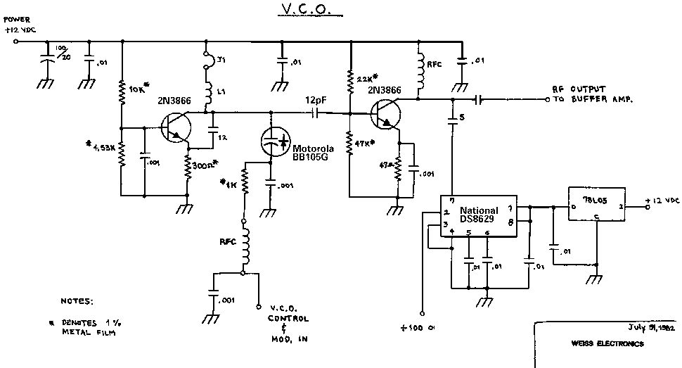
PLL Exciter

Schematic block diagram of the PLL. | Download Scientific Diagram